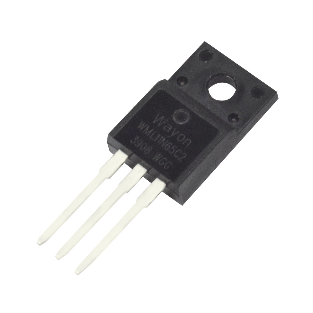
WML11N65C2 Super Junction Power MOSFET
WML11N65C2 Super Junction Power MOSFET
Couldn't load pickup availability
WML11N65C2 Super Junction Power MOSFET In the N layer of J-MOS, there is a P layer that is fashioned like a pillar. Alternating layers of P and N are aligned. Applying VDS causes the depletion layer to spread in the N-layer, but in SJ-MOS it does so differently than in regular D-MOS. (See illustrations of electric field intensity. The strength of the electric field reflects the condition of the depletion layer.) When it comes to D-MOS, the P/N layer contact has the strongest electric field intensity. Break-over phenomena (also known as breakdown phenomenon) occurs when the electric field intensity exceeds the limit of silicon, and this is the voltage limit. The electric field intensity in the N-layer is uniform for SJ-MOS, in contrast. As a result, an N- layer with lower resistance can be created for SJ-MOS, realizing. Its used in PC, Charger, LED TV, LCD TV Etc.
Features
-
Its drain to source voltage is 700V
-
Its used for power switching
-
It has lead free and halogen free construction
-
Low leakage current
-
It has the capability to improved dv/dT
- 100% avalanche energy rated
Specification
| Model | WML11N65C2 |
| Type | MOSFET |
| Package | TO-220F |
| VDS | 700V |
| Max reverse operating Voltage | 650V |
| Resistance | 0.47Ohm |
| No of pins | 3 |
| Operating and Storage Temperature Range | -55°C TO 150°C |
| Country of Origin | China |
Product features
Product features
Materials and care
Materials and care
Merchandising tips
Merchandising tips
Share


